Specializing in custom design applications, taking customer concepts from idea to final production.
Initially focused on the defense industry, Levanta has grown into the automotive, semiconductor, and optics and telecommunications fields. Levanta is expert at tool build, system retrofit and upgrade, programming and facilities build for process development, as well as engineering design, project management and vendor management.
Let’s Make It Happen
The industrial focus of these targeted industries and services originated through vacuum sciences: taking standard and proprietary processes, while respecting customer confidentiality, and designing, integrating and fabricating into production ready tools with, often with miultileven vacuum. Operating in the 10e-8 Torr range and often beyond, the systems have ranged in application from ultra-high vacuum process to “glove-box” nitrogen environment systems for inert cutting and welding and everything in between.
Levanta specializes in custom design applications, taking customer concepts from ideation to production. Applications range from thermal evaporation of metals and semiconductor materials, to sub-nanometer indium crystal formation for automotive industries.
A few of our customers

OUR EQUIPMENT RUNS 24/7 AROUND THE GLOBE.
Equipment Manufacturing
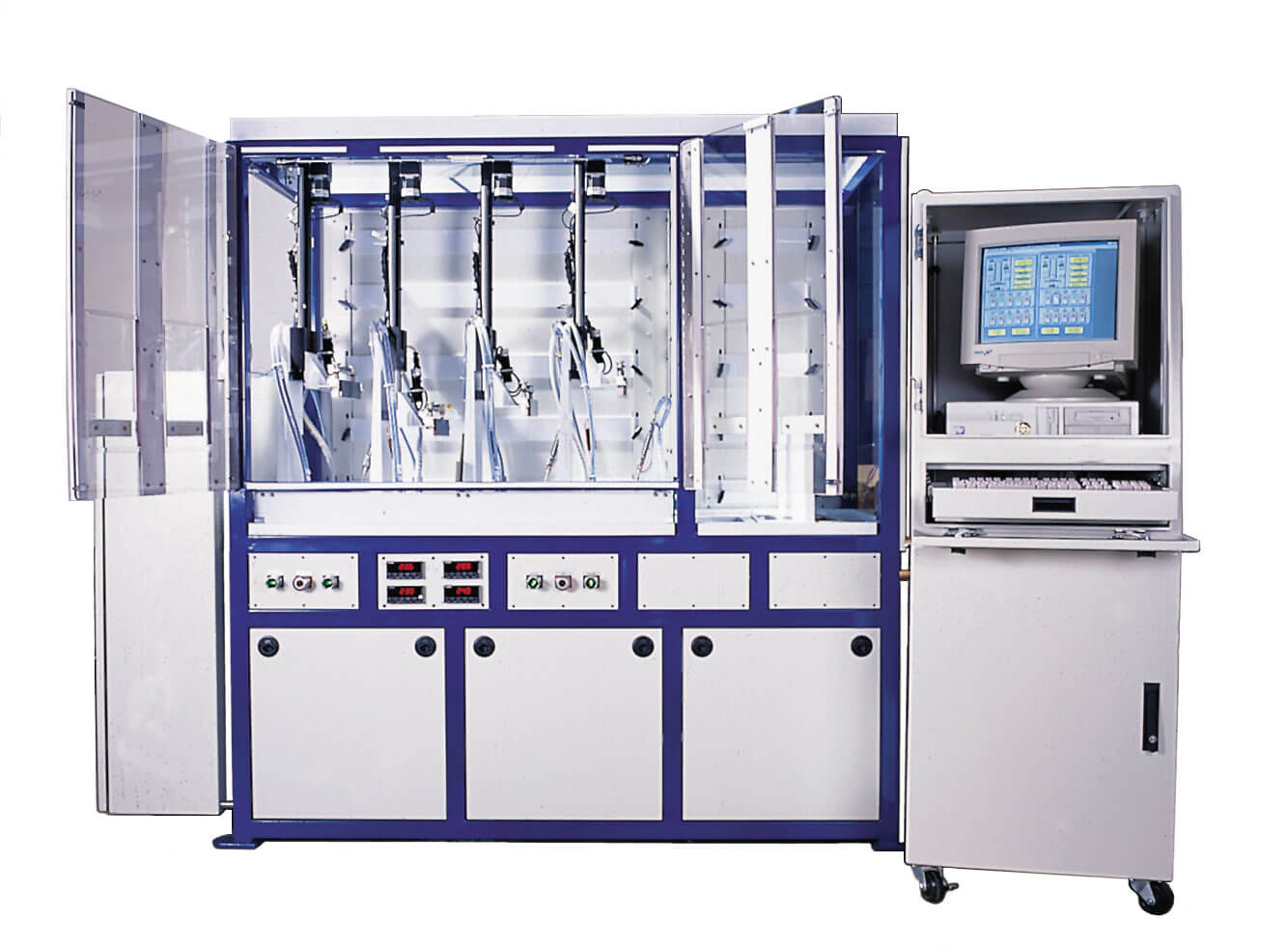
Glass Fiber Etching for Optical Telecom
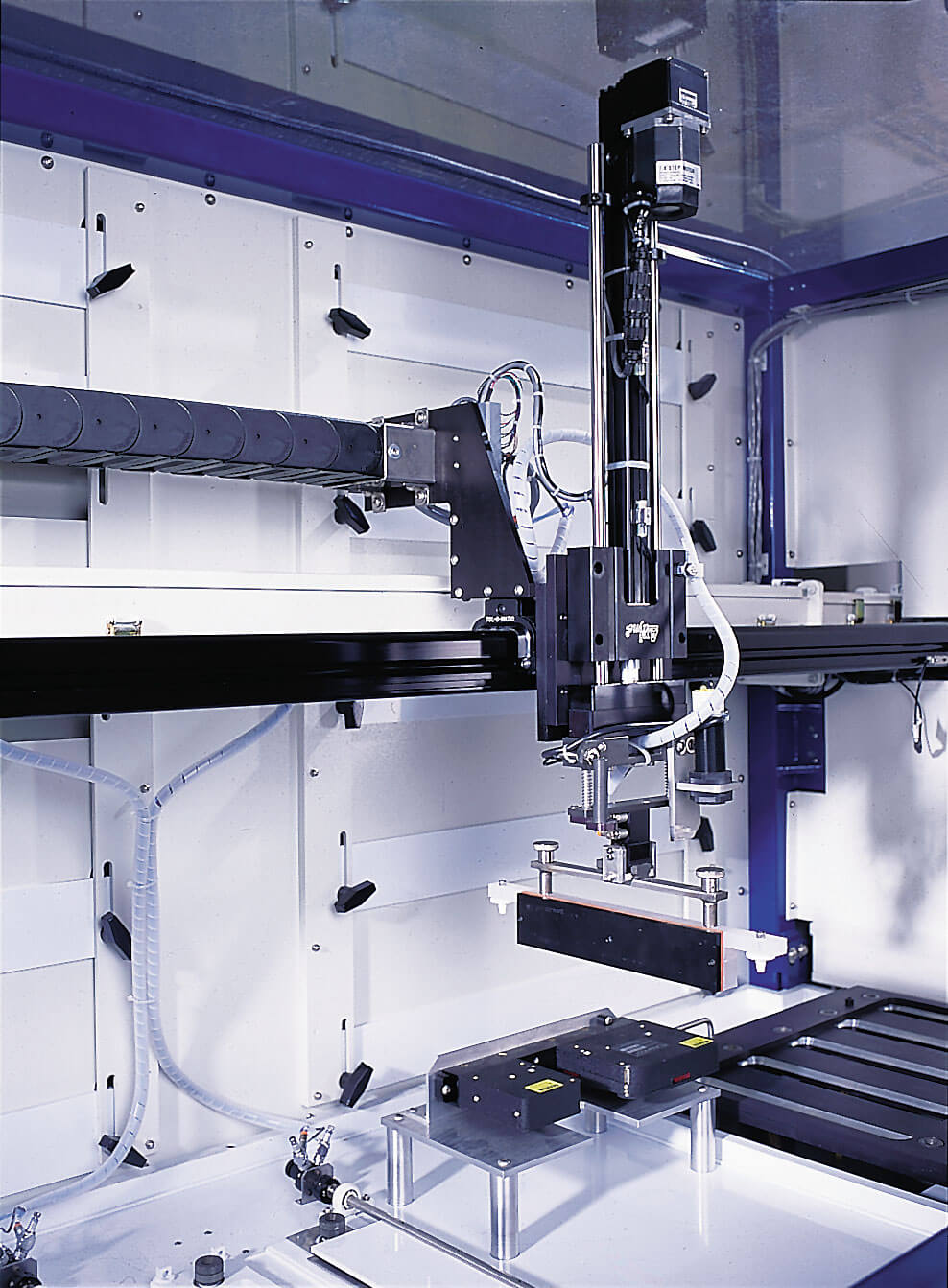
A multicomponent system based on an automated, four-station acid dip for cleaning fiber optics. Comprised of four stations, it has individual closed loop linear motion automation. Also, it has dual redundant closed loop temperature control circuits for maintaining sulfuric acid at a precise user controllable temperature.
Plating system machine
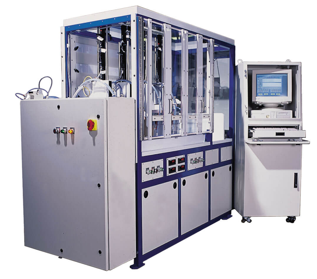
Custom system is an automated, 18 station electroless plating and coating system for glass fiber optics. This system electroplates Titanium, then Nickel then gold to allow fiber optic glass to be hermetically soldered to additional apparatus.
Particle Accelerator and Implanter (PIII)
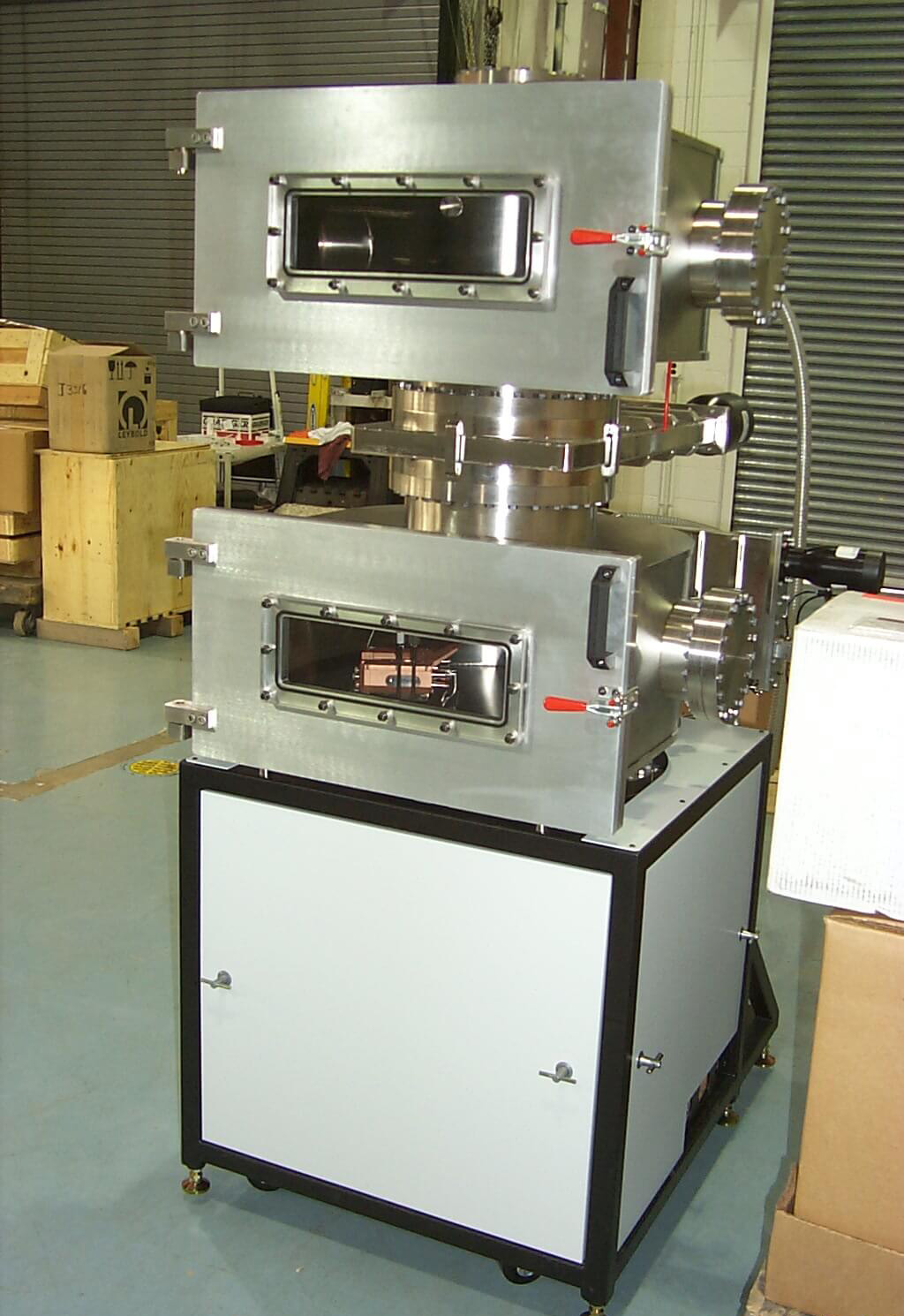
Custom application designed, built, and integrated, this ion implanter is used to accelerate hydrogen ions and to impact them into a target silicon wafer. These ions then quickly steal an electron from the substrate wafer and bond diatomically. The layer of hydrogen is precisely controlled to their aspect of depth penetration, resulting in a highly uniform, very thin cleavable layer. This layer of hydrogen is subsequently used as a cleave plane for separating a donor wafer from a product wafer, resulting in a Silicon On Insulator (SOI) wafer for semiconductor applications.
Vacuum Sputter Coating
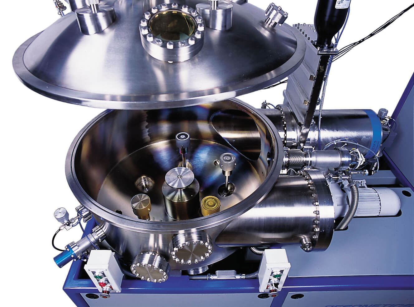
An alternative method to the electroless plater, this multicomponent system uses sputtering, which causes the transfer of metals through a vacuum, utilizing the conductive properties of an inert gas plasma. Although a higher initial cost, this method has no waste water, no heavy metal contamination, and no environmental impact, which less-expensive plating machines do have.
Contact Us
Let’s Make It Happen
Engineering
7 Scott Road, Unit #5, Hampton, NH. 03842
(603) 661-1166
Corporate
201 S. Denver Avenue, Suite 300 TULSA, OK 74103
(918) 583-9900
Fabrication & Testing
3152 Presidential Drive, Fairborn, Ohio 45324
(937) 320-9444
